I frequently come up with ideas for projects. If I really like the idea, I draw up the schematic and then maybe breadboard it. If I think the idea might be useful I normally try to make something a bit more permanent. This is fine for through hole devices - a slab of vero board, a couple of components from my through hole collection and away we go, however it is not so great for SMD circuits. I decided I needed to build and SMD prototype board.
I’ve been enticed into trying out SMD designs, partly because there is a better range of components, partly because the designs are smaller and mostly because it’s a new challenge. SMD designs are all well and good, but they makes bread boarding extremely difficult and more or less require a custom PCB every time you want to mock up a design. I could make the boards myself, but as I’m studying full time I don’t have all the time in the world so the decision is normally to try and buy one. What tends to happen then is I do the sums and realise that I don’t really need to spend 40 quid to make some transistor logic gates, and the project gets filed away.
A few days ago it hit me… the thing that’s missing in my life is an SMD prototype PCB, basically an “SMD breadboard”. After some ebay searching and a bit of head scratching I realised that there wasn’t much out there that I would actually like to pay for. So I decided to design one myself.
Specification
The first thing I did was sit down and try to work out what I wanted from the PCB. The basic idea is to build an SMD Prototype PCB that can be used flexibly either as a breadboard / breakout, or as a PCB in its own right. SMD parts can be soldered to it and prototype circuits built. The eventual design concept I came up with was:
- Breadboard compatible
- Footprints for several SOIC 300 chips
- Prototyping area for through hole components
- ICSP and XTAL connectors for one of the SOIC footprints
- A place for one 0805 chip on each SOIC pin
The Design
With the specification on board, I set about routing the board. I started using a Schematic and converting this into a PCB, but in the end ditched the schematic and just worked on the PCB manually. The Rev A design I came up with is shown below:
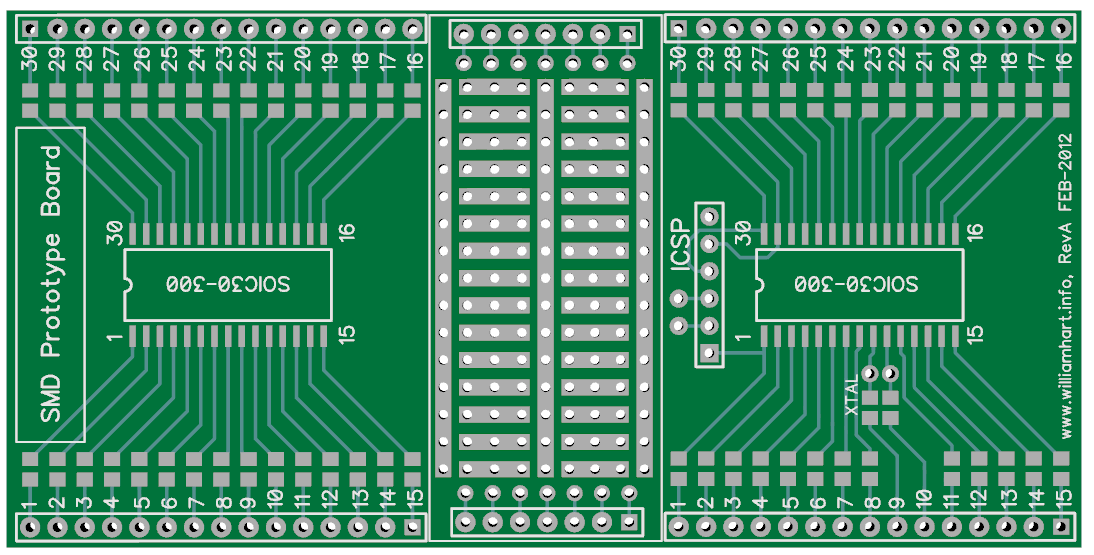
I decided to use the 0805 footprints on each SOIC pin as a solder jumper if no component is required. In practice, this requires either a 0 ohm resistor on the pad, or a bit of wire as a solder jumper. I also pulled the solder mask back on the through hole area to match the approach of a copper clad vero board.
Usage
The basic idea is to solder your components on the footprint and then hookup with jumper wire where its needed. I’ve tried to find a balance in the design between pre wired connections and flexibility.
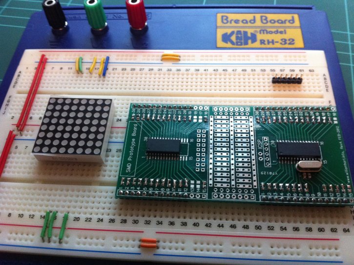
The image above shows the board with a PIC 28 pin device and a 24 pin 16 channel LED driver. There is a slight misalignment between the two SOIC sections meaning it takes a second or two to push it into the breadboard. I’m about to wire this one up to control the LED matrix via the LED driver.